PCB PCBA DFMA (DFM, DFT) And DFT Analysis
Argus (AESPL) is one of the leading PCB and system-level design and design analysis Company offering Design for Excellence (DFX) analysis services which includes Design for manufacturing (DFM), Design for Assembly (DFA) and Design for Testability ( DFT) analysis for applications like Space, Avionics, Telecom, Industrial, Medical, Computing, and Automotive.
Many companies do not have in-house expertise for Design for Excellence (DFX) Analysis and the companies that do have the expertise may experience peak overloads that require periodic outsourcing. Argus quick turn DFX (DFM, DFA, DFT) analysis services address the needs of these customers by providing expert resources at affordable prices. Application of Design for Excellence (DFX) analysis method results in shorter assembly time, lower assembly cost, elimination of process waste and increased product reliability.
Design for Excellence (DFX) Analysis Advantages
- Fewer revision spins per design.
- Fewer major production issues During manufacturing process.
- Avoid costly design changes and re-spins that delay project delivery
- Reduced time to market and increased on-time shipment commitments
- Reduced overall cost of test
- Use the right type of test depending on your process capability
- Align test strategy with defect opportunities.
- Reduced overall repair costs across process and product verification
- Process faults are detected earlier and with improved diagnostics
- Reduced PCB scrap and recycling costs
Design for Manufacturability (DFM) Analysis
- Design for Manufacturing (DFM ) process compiles PCB layout topology to reduce problems that can be encountered during the PCB fabrication processes required to manufacture an electronic system.
- After Design for Manufacturing (DFM ) Analysis is completed, a report is created including all the issues observed in analysis which is shared to designer for resolving the issues where these Issues are categorized into Critical/hot/warm/info priorities.
- DFM Analysis Includes: Net list Verification, Drill, Copper Layers, Solder Mask, Solder Paste, Silk Screen and Fabrication Layer Analysis.
Design for Assembly (DFA) Analysis
- Design for Assembly (DFA) Analysis is a process where the Gerber's that are being released to FAB house and BOM being released to Component Engineering team are Validated to check whether both are in Sync with each other.
- DFA checks allows user to confirm whether the PCB Assembly house is capable enough to assembly the board with special requirements that we have. DFA Analysis Environment includes Parts creation as well Validation tools.
- After Design for Assembly (DFA) Analysis a report is created including all the issues observed in analysis which is shared to designer for resolving the issues where these Issues are categorized into Critical/hot/warm/info priorities. DFA analysis includes below parameters.
- Footprint analysis
- BOM merge report
- Library merge report
- Component analysis
- Pad-stack analysis
- Solder paste analysis
- Pin to pad analysis

Design for Testability (DFT) Analysis
- DFT process of supplements the PCB's operational design with elements such as test points to facilitate the functional testing of the board. This added test points help the designer to check for functionality tests after the physical manufacturing process is over.
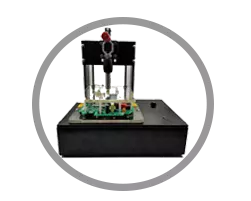
- Design for Testability is a specific post-layout process in which The CAD file is loaded in DFT Tool, and a mechanical analysis is performed in order to identify the physical access restrictions for In-Circuit or Flying probe test.
- DFT must be considered earlier and as part of the complete workflow, not just for probe placement. By verifying the testability at all stages, we can ensure the highest level of test quality for the minimum test cost.
- Part Proximity Error due to Body Clearance
- Power Nets Access Review
- Inaccessible pin
- Inaccessible Parts
- Test Point Size Review
- Nail Rules are Used to determine a test node’s accessibility priority